
Advanced chiplet architectures place increasing demands on the power delivery network (PDN). As multiple semiconductor dies are integrated within a single package, supplying high current at low voltage becomes a critical design challenge. Ferric's integrated voltage regulators (IVRs) enable compact, high-density power conversion close to the load, supporting efficient power distribution in advanced 2.5D and 3D semiconductor packaging architectures.
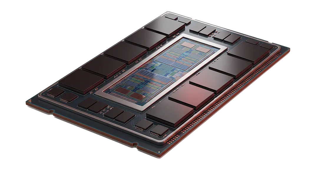
Chiplet power delivery refers to the architecture used to distribute and regulate electrical power across multiple semiconductor dies integrated within a single package.
Unlike monolithic processors, chiplet-based systems combine separate compute, I/O, memory-interface, and other functional dies through advanced packaging and high-bandwidth interconnects. These components may operate at different voltages, draw different amounts of current, and exhibit different transient load characteristics.
The power delivery network must provide stable voltage to each required power domain while managing resistive losses, parasitic inductance, package routing constraints, and thermal limitations.
As chiplet-based processors increase in complexity, the electrical path between the voltage regulator and the consuming die becomes increasingly important.
Conventional board-level voltage regulation typically requires low-voltage, high-current power to travel through PCB copper, package connections, and substrate routing before reaching the load.
In advanced multi-die packages, this introduces several constraints:
IR Drop: High current flowing through the resistance of the PDN produces voltage loss and dissipates power as heat.
Parasitic Inductance: Package and interconnect inductance contributes to transient voltage deviations during rapid changes in current demand.
Power Density: Multiple dies and high-bandwidth interconnects compete for limited package area and routing resources.
Multiple Voltage Domains: Different chiplets or functional blocks may require independent supply rails with distinct voltage and current requirements.
Thermal Constraints: Power conversion losses and concentrated heat sources must be considered alongside processor cooling and package reliability.
These challenges make power delivery a package-level design consideration rather than a problem that can be solved entirely at the motherboard.
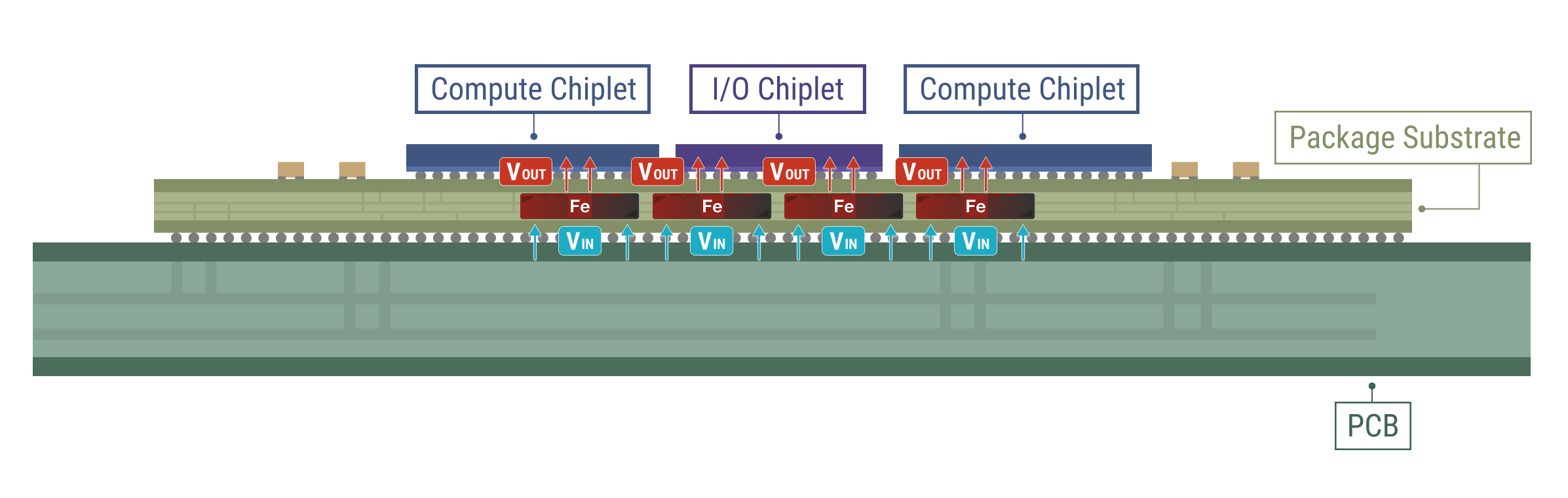
Ferric addresses these challenges by moving high-density DC-DC voltage conversion closer to the processor load.
Ferric IVRs integrate power switches, control circuitry, capacitors, and proprietary thin-film magnetic inductors into compact, multi-phase power converters. This reduces the footprint associated with conventional discrete voltage regulation and provides additional flexibility for package-level integration.
Shorter Power Delivery Paths: Locating voltage regulation closer to the consuming die reduces the distance over which high current must travel. A shorter power path can lower PDN resistance and inductance, reducing conduction losses and improving voltage regulation during rapid load changes.
High-Density Power Conversion: Ferric's integrated magnetic technology enables high-frequency, multi-phase voltage regulators with high current density. Compact power converters allow designers to evaluate power-delivery placements that would be difficult to implement with conventional discrete inductors and power stages.
Flexible Power Architecture: Multi-die packages may require several power rails with different load profiles. Ferric's IVR portfolio provides compact, single-output high-current converters and multi-output solutions that can be selected according to system requirements.
Regulator placement, device selection, current distribution, and rail configuration depend on the electrical and mechanical constraints of the package.
Ferric supports multiple power converter integration approaches, allowing power delivery to be optimized for different processor and package architectures.
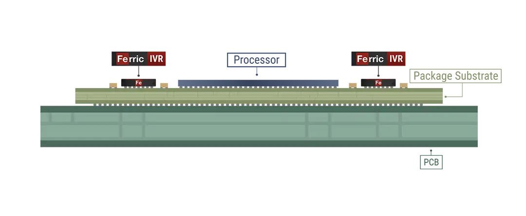
Ferric IVRs can be positioned adjacent to the processor die within the package, shortening the distance between voltage conversion and the load.
This approach can reduce the need to distribute high current over longer board-level paths while accommodating package-specific routing and mechanical constraints.
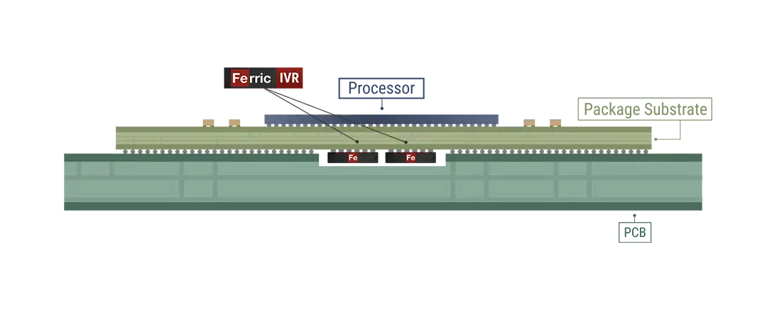
IVRs can also be placed on the land side of the processor package, bringing power conversion underneath the load.
Ferric's dual-sided IVR architecture further supports vertical power delivery by providing input and output connections on opposite surfaces of the converter.
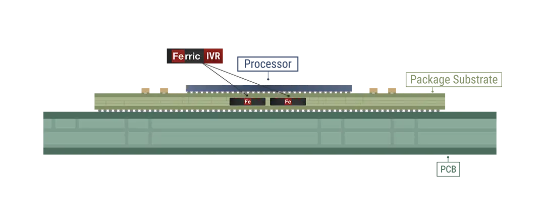
Embedding voltage regulation within the package substrate offers another approach to reducing the electrical distance between power conversion and the load.
The feasibility of embedded integration depends on substrate construction, available area, electrical connectivity, thermal requirements, and manufacturing processes.
Selecting a power architecture for a chiplet-based processor requires evaluating more than regulator efficiency or maximum output current.
Engineers must consider the current demand of each power domain, allowable voltage tolerance, load-step behavior, and target PDN impedance. Package resistance and inductance, decoupling capacitor placement, power and ground routing, and regulator control response all influence voltage stability at the die.
Thermal design is equally important. The location of the power converter must be compatible with package cooling, assembly processes, and long-term reliability requirements.
Ferric works with engineering teams to evaluate integration approaches based on processor power requirements, package constraints, and electrical performance targets.
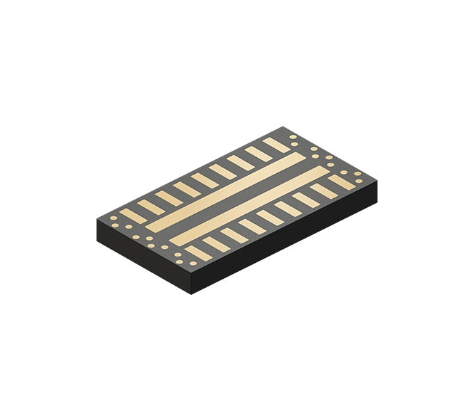
The Ferric Fe1766 is a 16-phase integrated buck converter delivering up to 160A of steady-state output current from a 35.5 mm² footprint, achieving 4.5 A/mm² current density.
Its integrated powertrain and compact form factor make it suitable for evaluating high-current package-level power delivery architectures. The Fe1766 also supports parallel operation of multiple devices for applications requiring higher aggregate current.
Thermal design is equally important. The location of the power converter must be compatible with package cooling, assembly processes, and long-term reliability requirements.
Ferric works with engineering teams to evaluate integration approaches based on processor power requirements, package constraints, and electrical performance targets.
Explore Fe1766 →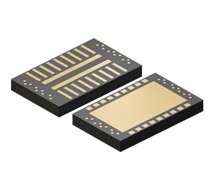
The Ferric Fe1767 Newport delivers up to 145A of steady-state output current in a 49.8 mm² package.
Its dual-sided architecture places VIN and VOUT connections on opposite sides of the device, enabling a direct vertical power path through the converter.
This configuration supports land-side power delivery approaches that reduce the distance between voltage regulation and the processor load.
Explore Fe1767 Newport →Advanced AI accelerators, GPUs, custom ASICs, and high-performance processors increasingly use heterogeneous integration to combine multiple functional dies within a single package.
These architectures place substantial demands on package power distribution, particularly when high-current compute dies operate alongside dense interconnects and other components with different power requirements.
High-density integrated voltage regulation offers a way to move the final stage of power conversion closer to the consuming dies, reducing reliance on long, low-voltage, high-current distribution paths.
The appropriate solution depends on the processor architecture, package topology, power requirements, and integration constraints.


We build the world's smallest, most efficient power converters. They power the future of computing and all digital electronics.